For a time, each new processor churned out more waste heat than the last. Had these chips kept on the trajectory they were following in the early 2000s, they would soon have packed about 6,400 watts onto each square centimeter—the power flux on the surface of the sun.
Things never got that bad because engineers worked to hold down chip power consumption. Data-center system-on-chip (SoC) designs are consistently second only to supercomputer processors in terms of performance, yet they typically consume only about 200 to 400 watts per square centimeter. The chip encased inside that smartphone in your pocket typically draws around 5 W.
Nevertheless, while computer chips won't burn a literal hole in your pocket (though they do get hot enough to fry an egg), they still require a lot of current to run the applications we use every day. Consider the data-center SoC: On average, it's consuming 200 W to provide its transistors with about 1 to 2 volts, which means the chip is drawing 100 to 200 amperes of current from the voltage regulators that supply it. Your typical refrigerator draws only 6 A. High-end mobile phones can draw a tenth as much power as data-center SoCs, but even so that's still about 10–20 A of current. That's up to three refrigerators, in your pocket!
Delivering that current to billions of transistors is quickly becoming one of the major bottlenecks in high-performance SoC design. As transistors continue to be made tinier, the interconnects that supply them with current must be packed ever closer and be made ever finer, which increases resistance and saps power. This can't go on: Without a big change in the way electrons get to and from devices on a chip, it won't matter how much smaller we can make transistors.

Fortunately, we have a promising solution: We can use a side of the silicon that's long been ignored.
Electrons have to travel a long way to get from the source that is generating them to the transistors that compute with them. In most electronics they travel along the copper traces of a printed circuit board into a package that holds the SoC, through the solder balls that connect the chip to the package, and then via on-chip interconnects to the transistors themselves. It's this last stage that really matters.
To see why, it helps to understand how chips are made. An SoC starts as a bare piece of high-quality, crystalline silicon. We first make a layer of transistors at the very top of that silicon. Next we link them together with metal interconnects to form circuits with useful computing functions. These interconnects are formed in layers called a stack, and it can take a 10-to-20-layer stack to deliver power and data to the billions of transistors on today's chips.
Those layers closest to the silicon transistors are thin and small in order to connect to the tiny transistors, but they grow in size as you go up in the stack to higher levels. It's these levels with broader interconnects that are better at delivering power because they have less resistance.

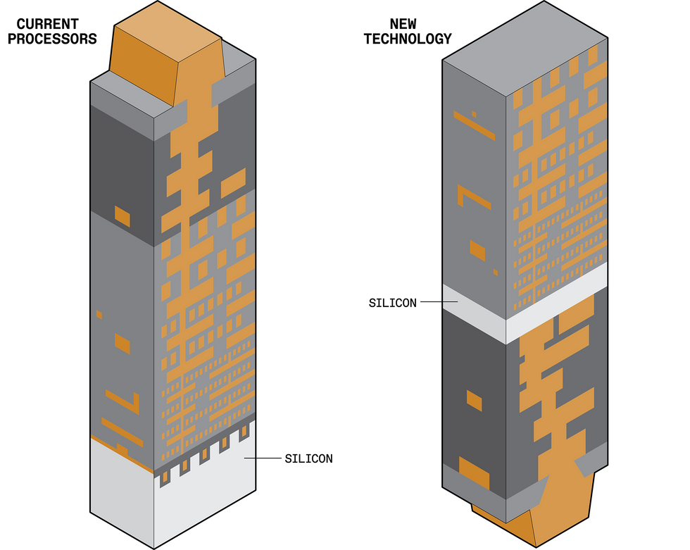
You can see, then, that the metal that powers circuits—the power delivery network (PDN)—is on top of the transistors. We refer to this as front-side power delivery. You can also see that the power network unavoidably competes for space with the network of wires that delivers signals, because they share the same set of copper resources.
In order to get power and signals off of the SoC, we typically connect the uppermost layer of metal—farthest away from the transistors—to solder balls (also called bumps) in the chip package. So for electrons to reach any transistor to do useful work, they have to traverse 10 to 20 layers of increasingly narrow and tortuous metal until they can finally squeeze through to the very last layer of local wires.
This way of distributing power is fundamentally lossy. At every stage along the path, some power is lost, and some must be used to control the delivery itself. In today's SoCs, designers typically have a budget that allows loss that leads to a 10 percent reduction in voltage between the package and the transistors. Thus, if we hit a total efficiency of 90 percent or greater in a power-delivery network, our designs are on the right track.
Historically, such efficiencies have been achievable with good engineering—some might even say it was easy compared to the challenges we face today. In today's electronics, SoC designers not only have to manage increasing power densities but to do so with interconnects that are losing power at a sharply accelerating rate with each new generation.
You can design a back-side power delivery network that's up to seven times as efficient as the traditional front-side network.
The increasing lossiness has to do with how we make nanoscale wires. That process and its accompanying materials trace back to about 1997, when IBM began to make interconnects out of copper instead of aluminum, and the industry shifted along with it. Up until then aluminum wires had been fine conductors, but in a few more steps along the Moore's Law curve their resistance would soon be too high and become unreliable. Copper is more conductive at modern IC scales. But even copper's resistance began to be problematic once interconnect widths shrank below 100 nanometers. Today, the smallest manufactured interconnects are about 20 nm, so resistance is now an urgent issue.
It helps to picture the electrons in an interconnect as a full set of balls on a billiards table. Now imagine shoving them all from one end of the table toward another. A few would collide and bounce against each other on the way, but most would make the journey in a straight-ish line. Now consider shrinking the table by half—you'd get a lot more collisions and the balls would move more slowly. Next, shrink it again and increase the number of billiard balls tenfold, and you're in something like the situation chipmakers face now. Real electrons don't collide, necessarily, but they get close enough to one another to impose a scattering force that disrupts the flow through the wire. At nanoscale dimensions, this leads to vastly higher resistance in the wires, which induces significant power-delivery loss.
Increasing electrical resistance is not a new challenge, but the magnitude of increase that we are seeing now with each subsequent process node is unprecedented. Furthermore, traditional ways of managing this increase are no longer an option, because the manufacturing rules at the nanoscale impose so many constraints. Gone are the days when we could arbitrarily increase the widths of certain wires in order to combat increasing resistance. Now designers have to stick to certain specified wire widths or else the chip may not be manufacturable. So, the industry is faced with the twin problems of higher resistance in interconnects and less room for them on the chip.
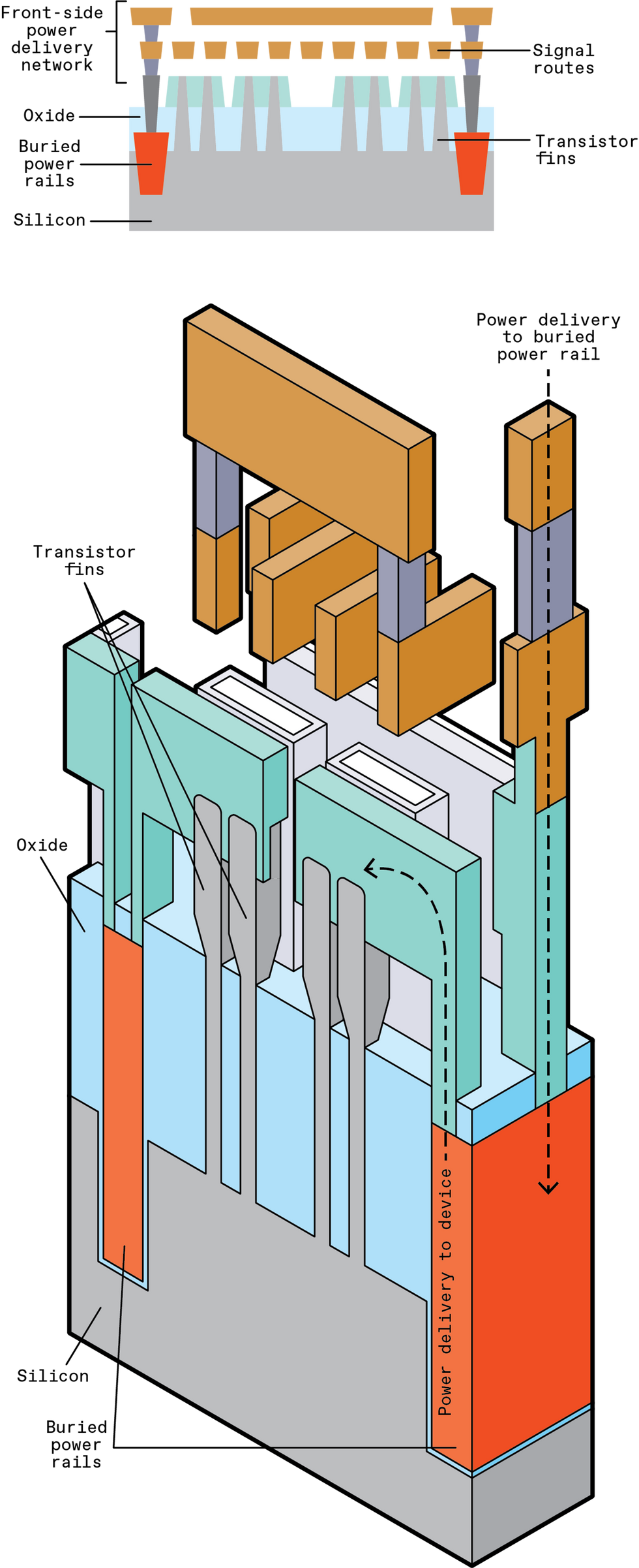
There is another way: We can exploit the "empty" silicon that lies below the transistors. At Imec, where authors Beyne and Zografos work, we have pioneered a manufacturing concept called "buried power rails," or BPR. The technique builds power connections below the transistors instead of above them, with the aim of creating fatter, less resistant rails and freeing space for signal-carrying interconnects above the transistor layer.

To build BPRs, you first have to dig out deep trenches below the transistors and then fill them with metal. You have to do this before you make the transistors themselves. So the metal choice is important. That metal will need to withstand the processing steps used to make high-quality transistors, which can reach about 1,000 °C. At that temperature, copper is molten, and melted copper could contaminate the whole chip. We've therefore experimented with ruthenium and tungsten, which have higher melting points.
Since there is so much unused space below the transistors, you can make the BPR trenches wide and deep, which is perfect for delivering power. Compared to the thin metal layers directly on top of the transistors, BPRs can have 1/20 to 1/30 the resistance. That means that BPRs will effectively allow you to deliver more power to the transistors.
Furthermore, by moving the power rails off the top side of the transistors you free up room for the signal-carrying interconnects. These interconnects form fundamental circuit "cells"—the smallest circuit units, such as SRAM memory bit cells or simple logic that we use to compose more complex circuits. By using the space we've freed up, we could shrink those cells by 16 percent or more, and that could ultimately translate to more transistors per chip. Even if feature size stayed the same, we'd still push Moore's Law one step further.
Unfortunately, it looks like burying local power rails alone won't be enough. You still have to convey power to those rails down from the top side of the chip, and that will cost efficiency and some loss of voltage.
Gone are the days when we could arbitrarily increase the widths of certain wires in order to combat increasing resistance.
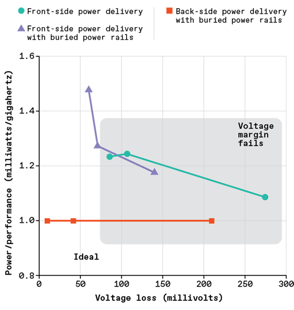
Researchers at Arm, including authors Cline and Prasad, ran a simulation on one of their CPUs and found that, by themselves, BPRs could allow you to build a 40 percent more efficient power network than an ordinary front-side power delivery network. But they also found that even if you used BPRs with front-side power delivery, the overall voltage delivered to the transistors was not high enough to sustain high-performance operation of a CPU.
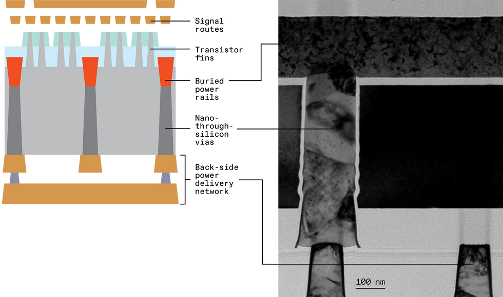
Luckily, Imec was simultaneously developing a complementary solution to further improve power delivery: Move the entire power-delivery network from the front side of the chip to the back side. This solution is called "back-side power delivery," or more generally "back-side metallization." It involves thinning down the silicon that is underneath the transistors to 500 nm or less, at which point you can create nanometer-size "through-silicon vias," or nano-TSVs. These are vertical interconnects that can connect up through the back side of the silicon to the bottom of the buried rails, like hundreds of tiny mineshafts. Once the nano-TSVs have been created below the transistors and BPRs, you can then deposit additional layers of metal on the back side of the chip to form a complete power-delivery network.
Expanding on our earlier simulations, we at Arm found that just two layers of thick back-side metal was enough to do the job. As long as you could space the nano-TSVs closer than 2 micrometers from each other, you could design a back-side PDN that was four times as efficient as the front-side PDN with buried power rails and seven times as efficient as the traditional front-side PDN.
The back-side PDN has the additional advantage of being physically separated from the signal network, so the two networks no longer compete for the same metal-layer resources. There's more room for each. It also means that the metal layer characteristics no longer need to be a compromise between what power routes prefer (thick and wide for low resistance) and what signal routes prefer (thin and narrow so they can make circuits from densely packed transistors). You can simultaneously tune the back-side metal layers for power routing and the front-side metal layers for signal routing and get the best of both worlds.

In our designs at Arm, we found that for both the traditional front-side PDN and front-side PDN with buried power rails, we had to sacrifice design performance. But with back-side PDN the CPU was able to achieve high frequencies and have electrically efficient power delivery.
You might, of course, be wondering how you get signals and power from the package to the chip in such a scheme. The nano-TSVs are the key here, too. They can be used to transfer all input and output signals from the front side to the back side of the chip. That way, both the power and the I/O signals can be attached to solder balls that are placed on the back side.
Simulation studies are a great start, and they show the CPU-design-level potential of back-side PDNs with BPR. But there is a long road ahead to bring these technologies to high-volume manufacturing. There are still significant materials and manufacturing challenges that need to be solved. The best choice of metal materials for the BPRs and nano-TSVs is critical to manufacturability and electrical efficiency. Also, the high-aspect-ratio (deep but skinny) trenches needed for both BPRs and nano-TSVs are very difficult to make. Reliably etching tightly spaced, deep-but-narrow features in the silicon substrate and filling them with metal is relatively new to chip manufacture and is still something the industry is getting to grips with. Developing manufacturing tools and methods that are reliable and repeatable will be essential to unlocking widespread adoption of nano-TSVs.
Furthermore, battery-powered SoCs, like those in your phone and in other power-constrained designs, already have much more sophisticated power-delivery networks than those we've discussed so far. Modern-day power delivery separates chips into multiple power domains that can operate at different voltages or even be turned off altogether to conserve power. (See " A Circuit to Boost Battery Life," IEEE Spectrum, August 2021.)

Thus, back-side PDNs and BPRs are eventually going to have to do much more than just efficiently deliver electrons. They're going to have to precisely control where electrons go and how many of them get there. Chip designers will not want to take multiple steps backward when it comes to chip-level power design. So we will have to simultaneously optimize design and manufacturing to make sure that BPRs and back-side PDNs are better than—or at least compatible with—the power-saving IC techniques we use today.
The future of computing depends upon these new manufacturing techniques. Power consumption is crucial whether you're worrying about the cooling bill for a data center or the number of times you have to charge your smartphone each day. And as we continue to shrink transistors and ICs, delivering power becomes a significant on-chip challenge. BPR and back-side PDNs may well answer that challenge if engineers can overcome the complexities that come with them.
This article appears in the September 2021 print issue as "Power From Below."
"chips" - Google News
August 25, 2021 at 02:00PM
https://ift.tt/3sNlpj7
Next-Gen Chips Will Be Powered From Below - IEEE Spectrum
"chips" - Google News
https://ift.tt/2RGyUAH
https://ift.tt/3feFffJ
Bagikan Berita Ini


0 Response to "Next-Gen Chips Will Be Powered From Below - IEEE Spectrum"
Post a Comment