Ayar Labs, a startup developing optical interconnects for data centers and supercomputers, has landed $35 million in its latest round of funding. The startup said that it would use the proceeds to roll out its in-package silicon photonics technology, which enables processors and memory in servers and other areas to communicate with each other using light.
The funding brings the Santa Clara, California-based company's haul to more than $60 million since it was founded in 2015. The funding was led by Downing Ventures and BlueSky Capital, while other investors in the round included Applied Ventures, the investment arm of Applied Materials, as well as Intel Capital, Globalfoundries, Lockheed Martin, and Playground Global.
The startup is trying to transform its optical interconnects into a major component of any system that moves a massive amount of data, including in cloud data centers and colossal supercomputers. Other areas the company is targeting in the future include aerospace and defense systems, 5G networks, and lidar sensors slapped on the sides of autonomous cars.
Today, cloud computing vendors and other titans of the technology industry, such as Google, Microsoft and Amazon, use optical connections in data centers to lash together servers and to connect data centers over long-range cables. But they could use server chips with Ayar's silicon photonics inside to increase the amount of data these systems can process even further.
In data centers and supercomputers, data travels constantly while it is processed. Data moves from central processing units (CPUs) to memory to other types of server processors, including graphics processing units (GPUs) that handle deep learning and other workloads. The constant movement means that the time it takes to carry out computing chores depends on the speed of the wires. Today, the data dashes from one chip to another electronically, through copper wires.
But as the performance of processors in servers has soared over the last decade, the electronic interconnects moving data from the memory to the central processor and other chips in servers have struggled to keep pace. The bandwidth of the copper wires has become the bottleneck to improving performance, power, area and cost in data centers and supercomputers. But solving it could also open the door to new system architectures, which are constrained by copper wires.
Ayar said that its interconnect chips promise to speed up data transfers by moving data from memory to the processor and other components in the server using photons of light, which are faster and more energy-efficient than electrons. The startup said the chips bring improvements of up to 1000 times in throughput compared to traditional copper wires, increasing the system-level performance. Sending data over fiber optics consume up to 10 times less power, it says.
Ayar's technology is based on a decade of research at MIT, UC Berkeley, and the University of Colorado at Boulder, with funding from DARPA, the Department of Defense's research division.
The company's flagship chip, TeraPHY, integrates all the optical and electronic technology on a single, compact silicon die. Available as a chiplet, the slab of silicon can be incorporated on the same package as a central processing unit or server networking chip to give it high-speed data transmission capabilities. The chip communicates with the CPU and other ICs in the package over a standard interface. That way, the chips act as though they are sharing the same die.
The networking chip is based on a novel architecture with eight ports or "light channels" capable of transferring up to tens of trillions of bits of data per second directly out of the processors on the package, translating the light into electronic signals that other server gear can understand. Each port has around the same bandwidth as eight PCIe Gen 5 connections, the startup said.
There are lots of potential advantages to its in-package silicon photonics. The IC could be used to replace more of the copper cables that cloud and other technology giants use to wire vast warehouses of servers, saving money. By replacing bulky networking gear, it could also save space and cut power in servers. The bandwidth boost Ayar is promising could also open the door to more densely packed server clusters that can be cooled more efficiently than today.
The chip contains a die-to-die interface based on the open-source advanced interconnect bus, or AIB, to connect to central processors or other chips from partners within the same package.
The Silicon Valley startup is also winning over major players in the semiconductor industry with its in-package silicon photonics. Intel has partnered with it to integrate optical interconnects on CPUs and other server processors, as part of DARPA's PIPES program. Earlier in the year, Intel said that it had successfully co-packaged TeraPHY with one of its programmable FPGAs using its EMIB silicon-bridge packaging and AIB interface, giving it data transfer rates of up to 2 Tbps.
One way it stands out from rivals is in manufacturing the chip on industry-standard production lines, speeding up its time-to-market. The chip is based on a 45-nm node from Globalfoundries. Early in the year, it started rolling out sample products to chip suppliers, server manufacturers, telecom equipment vendors, and others to cement relationships with early potential customers.
CEO Charles Wuischpard said that it would use the funding to accelerate the development of its in-package optical interconnect devices as well as expand the company's international footprint.
What you’ll learn:
- How to maximize storage life by decreasing write amplification factor (WAF).
- How the address-mapping choice can make a big difference to the WAF.
- How the appropriate flash-management firmware can assist with the above.
Flash memory is organized in a hierarchy of blocks, pages, and cells. In the older single-level-cell (SLC) devices, each cell stores only one bit of information. With the newer multi-level-cell (MLC) memory, pages are typically between 8 and 16 kB. Blocks can be up to 8 MB.
When it comes to NAND flash, data is written a page at a time. However, only whole blocks can be erased. To ensure this is carried out correctly, the flash controller uses mapping algorithms to process exactly where data should be sent on the NAND flash.
This mapping data manages the blocks and pages and allocates them for subsequent use. Flash-controller mapping involves lots of complex algorithms and ultimately ensures that wear and tear is carried out evenly. If wear occurs evenly, it helps ensure drive longevity and optimizes flash management.
Write Amplification Factor
Rewriting data to an SSD significantly affects endurance. An important parameter for tracking the lifetime and endurance of a storage device is the write amplification factor (WAF). There’s one important element to remember with the WAF: the smaller, the better.
The WAF tallies the number of writes made to the flash memory and then performed by the host. Extra writes may be needed for functions such as erasing blocks before data is written. The extra writes could indicate a mismatch between the data amount and the page size.
For example, a sequential write of 4 kB of data to a flash memory where the page size is 16 kB will result in a WAF of 4, because the entire page must be written (4 kB four times in a row to total 16 kB). Since a partial block erase isn’t possible, it’s important for the algorithm to take the mapping of the whole block into consideration.
Block-Based mapping
In any flash storage system, the controller must manage the mapping from the logical addresses used by the host operating system to flash memory physical addresses. A simple, however arguably outdated, method commonly used is block-based mapping, in which a one-to-one mapping occurs between addresses within logical and physical blocks (Fig. 1).
 1. Flash-memory controllers often employ block-based mapping.
Managing in this way causes logical page 1 to always map to physical page 1 in a block, although this can be in any block.
The address-mapping choice can make a big difference to the WAF. In the case of block-based mapping, write amplification can be enormous, especially for small random writes. If a block must be erased to accommodate a single sector write, the WAF can increase to 2000 because adding the new data initiates copying the entire block of previous content to a new block.
Certain SD cards designed for video recording still use block-based mapping due to the data patterns that involve many sequential writes and only erasing data once the card is written full. However, most applications have a greater need for performance.
Sub-Page Mapping
Page-based mapping is a more versatile logical-to-physical address-mapping method than block-based mapping. While logical pages are still mapped to physical pages, more flexibility is available because logical page 1 can now be mapped to any physical page within a block.
Sub-page-based mapping means that the address mapping is achieved at a level smaller than a page. Memory-allocation flexibility broadens with this technique. However, writes still must be done at the level of an entire page.
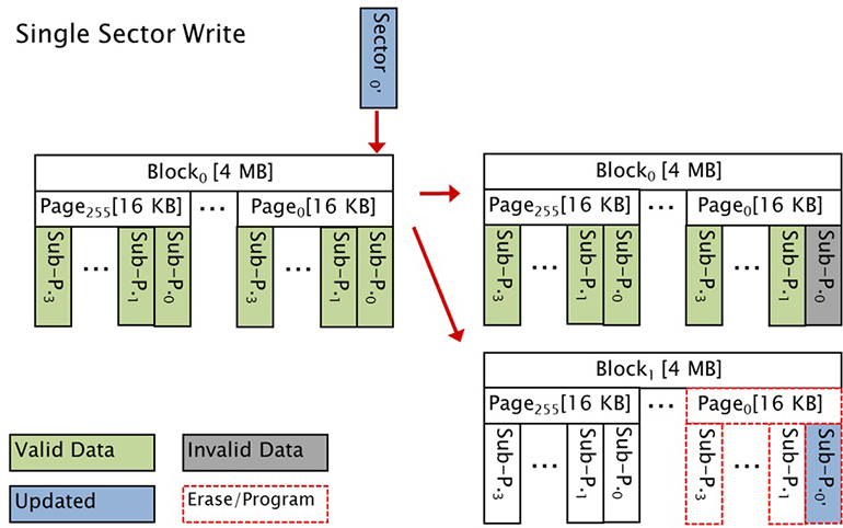
Sub-page-based mapping significantly reduces the WAF. Even if a block has to be erased because no unused block is available, only the new sector of data must be written to the new block. The old sector of data is marked as invalid, and the other data in that block stays put.
As a result, even in the worst-case scenario, the WAF is reduced to 16 compared with the 2000 mentioned earlier. By reducing the number of extra writes, sub-page-based mapping can significantly improve the lifetime of a drive.
For example, Hyperstone’s flash-management firmware, hyMap, implements an enhanced Flash Translation Layer (FTL) mapping that improves random write performance, reliability, and endurance (Fig. 2). Since many factors including the pattern of use affect the overall WAF, firmware can be compiled for different sub-page granularities and tuned to the expected usage model.
 2. Hyperstone’s hyMap firmware utilizes page-based mapping.
By increasing drive endurance and longevity, hyMap firmware and its sub-page-based mapping system enables cost savings in applications that have replaced older SLC designs with MLC memory designs.
Continuously optimizing flash-memory-controller mapping ensures higher performance, a lower WAF, and increased endurance. As a result, cost reduction, higher capacity, and greater competitiveness is possible.
Damien Col is Technical Marketing Manager at Hyperstone.
"chips" - Google News
November 20, 2020 at 06:26AM
https://ift.tt/35MEZC7
Startup Lands $35 Million to Roll Out Optical Interconnects for Chips - Electronic Design
"chips" - Google News
https://ift.tt/2RGyUAH
https://ift.tt/3feFffJ
Bagikan Berita Ini


0 Response to "Startup Lands $35 Million to Roll Out Optical Interconnects for Chips - Electronic Design"
Post a Comment