Scientists from the Institute of Computing Technology at the Chinese Academy of Sciences introduced an advanced 256-core multi-chiplet and have plans to scale the design up to 1,600-core chips that employ an entire wafer as one compute device.
It is getting harder and harder to increase transistor density with every new generation of chips, so chipmakers are looking for other ways to increase performance of their processors, which includes architectural innovations, larger die sizes, multi-chiplet designs, and even wafer-scale chips. The latter has only been managed by Cerebras so far, but it looks like Chinese developers are looking towards them as well. Apparently, they have already built a 256-core multi-chiplet design and are exploring ways to go wafer-scale, using an entire wafer to build one large chip.
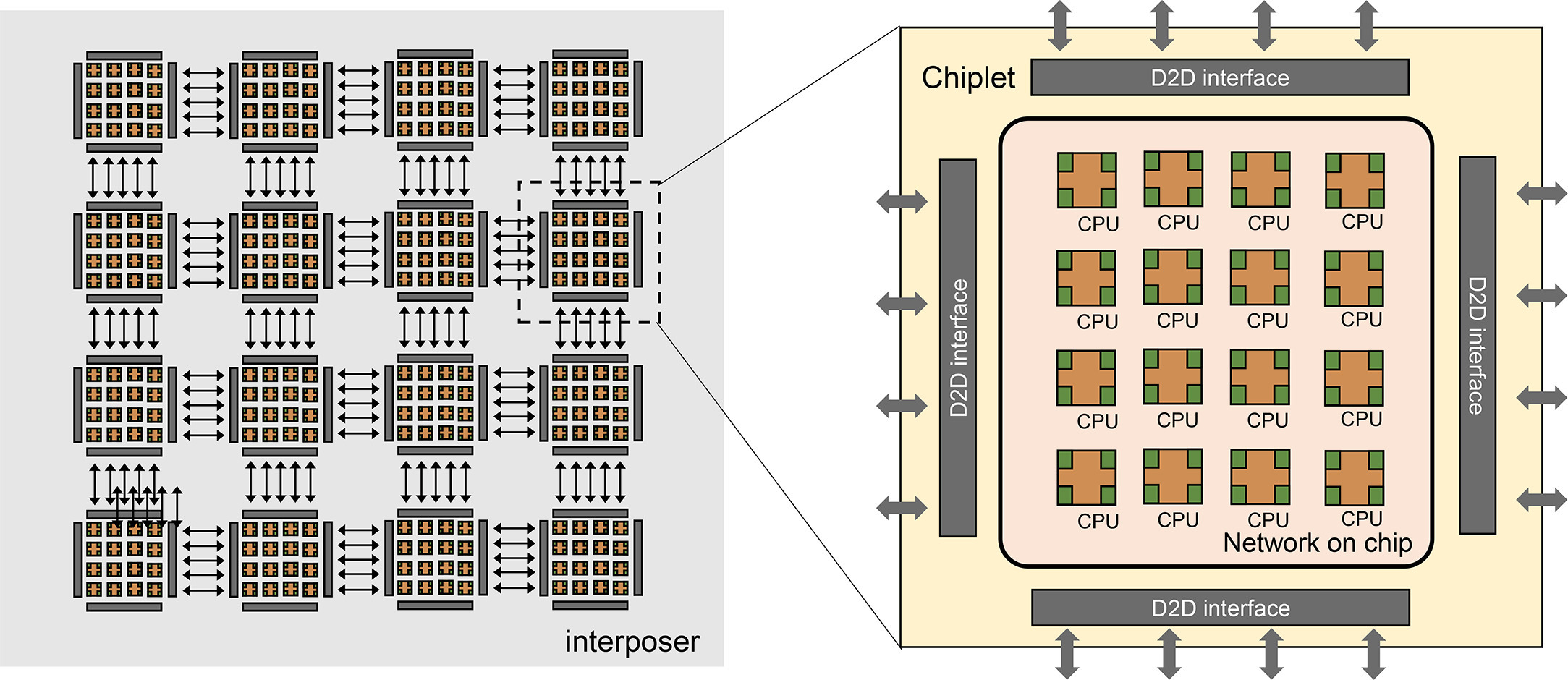
Scientists from the Institute of Computing Technology at the Chinese Ac ademy of Sciences introduced an advanced 256-core multi-chiplet compute complex called Zhejiang Big Chip in a recent publication in the journal Fundamental Research, as reported by The Next Platform. The multi-chiplet design consists of 16 chiplets containing 16 RISC-V cores each and connected to each other in a conventional symmetric multiprocessor (SMP) manner using a network-on-chip so that the chiplets could share memory. Each chiplet has multiple die-to-die interfaces to connect to neighbor chiplets over a 2.5D interposer and the CAS researchers say that the design is scalable to 100 chiplets, or to 1,600 cores.

Zhejiang chiplets are reportedly made on a 22nm-class process technology, presumably by Semiconductor Manufacturing International Corp. (SMIC). We are not sure how much power would a 1,600-core assembly interconnected using an interposer and made on a 22nm production node would consume. However, as The Next Platform points out, there is nothing that stops CAS to produce a 1,600-core wafer-scale chip, which would greatly optimize their power consumption and performance due to reduced latencies.
The paper explores the limits of lithography and chiplet technology and discusses the potential of this new architecture for future computing needs. Multi-chiplet designs could be used to build processors for exascale supercomputers, the researchers note, something that AMD and Intel do today.
"For the current and future exascale computing, we predict a hierarchical chiplet architecture as a powerful and flexible solution," the researchers wrote. “The hierarchical-chiplet architecture is designed as many cores and many chiplets with hierarchical interconnect. Inside the chiplet, cores are communicated using ultra-low-latency interconnect while inter-chiplet are interconnected with low latency beneficial from the advanced packaging technology, such that the on-chiplet latency and the NUMA effect in such high-scalability system can be minimized."
Meanwhile, the CAS researchers propose to use multi-level memory hierarchy for such assemblies, which could potentially introduce difficulties with programming of such devices.
"The memory hierarchy contains core memory [caches], on-chiplet memory and off-chiplet memory," the description reads. "The memory from these three levels vary in terms of memory bandwidth, latency, power consumption and cost. In the overview of hierarchical-chiplet architecture, multiple cores are connected through cross switch and they share a cache. This forms a pod structure and the pod is interconnected through the intra-chiplet network. Multiple pods form a chiplet and the chiplet is interconnect through the inter-chiplet network and then connects to the off-chip(let) memory. Careful design is needed to make full use of such hierarchy. Reasonably utilizing the memory bandwidth to balance the workload of different computing hierarchy can significantly improve the chiplet system efficiency. Properly designing the communication network resource can ensure the chiplet collaboratively performing the shared-memory task."
The Big Chip design could also take advantage of such things as optical-electronic computing, near-memory computing, and 3D stacked memory. However, the paper stops short of providing specific details on the implementation of these technologies or addressing the challenges they might pose in the design and construction of such complex systems.
Meanwhile, The Next Platform assumes that CAS has already built its 256-core Zhejiang Big Chip multi-chiplet compute complex. From here, the company can explore performance of its chiplet design and then make decisions regarding system-in-packages with a higher number of cores, different classes of memory, and wafer-scale integration.
"chips" - Google News
January 05, 2024 at 03:57AM
https://ift.tt/Ul6NVdM
China planning 1600-core chips that use an entire wafer — similar to American company Cerebras 'wafer-scale' designs - Tom's Hardware
"chips" - Google News
https://ift.tt/dM3ZJfB
https://ift.tt/pcm8CjY
Bagikan Berita Ini


0 Response to "China planning 1600-core chips that use an entire wafer — similar to American company Cerebras 'wafer-scale' designs - Tom's Hardware"
Post a Comment