Marvell Technology, trying to further transform itself into one of the world's largest vendors of network infrastructure chips, rolled out its latest line of Octeon networking chips to meet the throughput and latency demands of 5G telecom equipment. Marvell said it hammered out deals with telecom gear vendors, including Nokia and Samsung, to supply the Octeon chips for use in 5G base stations.
The company introduced the first chip in its latest generation of Octeon Fusion chips, the CNF95xx, which is targeted at the 5G infrastructure market. The chip incorporates a range of hardware accelerators for secure networking, baseband processors, and programmable DSP cores, ideal for 5G networks that offer far faster data transfers than 4G technology. Marvell said it is currently the only merchant silicon on the market for 5G base stations.
Marvell said the new Octeon Fusion chips pump out more performance per watt than its predecessors while also supporting the millimeter waves bands used in 5G networks. The chip can be used in macro base stations with antennas and other hardware that beam out signals over long distances. The chip can also be used for massive MIMO, which is used to transfer data through targeted 5G beams, speeding up data rates and lifting throughput.
The Santa Clara, California-based company is attempting to become a global powerhouse in chips used in 5G networking gear. Marvell is looking to gain ground with the world's top players, including Ericsson and Nokia, which accounted for more than 50% market share in 2018, according to Omdia. Ericsson and Nokia have largely built chips in-house in recent years or partnered with Broadcom, Marvell, or other firms to build base station silicon.
Marvell is competing against Intel, which is looking to become the global leader with 40% of the market share in base station chips by 2021. Intel has hammered out contracts with three major vendors of telecommunications equipment to supply its 10-nanometer Snow Ridge chip for 5G networking gear. Intel plans to start supplying it to Ericsson, Nokia, and ZTE, which hold the No. 2, No. 3 and No. 4 positions in the telecom market, respectively.
 (Image courtesy of Marvell).
The baseband modem is based on 42 programmable DSP cores that are crammed into the networking subsystem and connected to a range of hardware accelerators that handle the encoding and decoding of 4G LTE and 5G transmissions. The cores and accelerators are interlaced with a high-speed, multi-ported interconnect fabric and linked to 24 MB of memory cache shared over the company's high-speed crossbar interconnect (XBAR).
Marvell said the six-core Arm CPU is based on its TX2 architecture and clocked at 2.6 GHz. Each core contains more than 100 KB of internal memory to cache instructions or other information. Clusters of cores are attached to 1.25 MB of shared MLC cache. High-speed crossbar interconnects are used to connect all the cores to the memory subsystem, which integrates up to 3.5 MB of LLC cache and 2x memory controllers for DDR4 DRAM.
The chip incorporates 6x25G SerDes cores to connect the baseband processor and other accelerators to the radio components using the Radio-over-Ethernet (RoE) standard. The chip contains 4x25 SerDes cores that support up to 100 Gbps Ethernet as well as a range of other I/O interfaces. Marvell said it would roll out semi-custom Octeon Fusion to fit its customer's exact needs. It also allows customers to license the IP for custom ASICs.
The Silicon Valley company said it is supplying Octeon Fusion chips to Samsung, which plans to use it in 5G base stations. Marvell has a long-term partnership with Samsung to build out new generations of radio and control plane processors for both 4G LTE and 5G networks. Samsung has been one of the underdogs in the telecom equipment market in recent years, winning around 5% of the sales in the segment in 2018, according to Omdia.
But it is looking to leapfrog Ericsson, Nokia, Huawei, and others in rolling out the latest 5G networks. Samsung hopes to command 20% of the global market by the end of the year.
 (Image courtesy of Marvell).
Marvell is also giving its customers another weapon to wield in the fight against Huawei, the world's largest vendor of telecommunications gear with more than 30% market share in 2018, according to Omdia. Huawei has maintained its global lead in 5G technology in the face of the relentless pressure from the United States to suppress the rollout of its 5G network hardware. Huawei also depends on in-house chip designs for 5G base stations.
Marvell is winning over other major customers for its Octeon Fusion processors. Nokia, one of the global leaders in the telecommunications gear market, said that it plans to roll out base stations with its Octeon Fusion family of chips, which can handle the global range of frequency bands used by 5G technology, including millimeter waves. In March, Marvell also agreed to help plot out future generations of Nokia's 5G baseband ASICs.
“Marvell provides the industry’s most comprehensive set of 5G silicon solutions,” said Raj Singh, corporate vice president of the infrastructure and server processor business at Marvell. "And the Octeon Fusion family is the cornerstone of our architecture, providing a comprehensive, software-compatible, and customizable base station compute platform." More than 7 million Octeon Fusion chips are used in current 3G, 4G and 5G base stations.
Marvell also recently rolled out latest generation of infrastructure processors, Octeon TX2, which can be used in 4G and 5G networking devices as well as switches, gateways, routers, and other gear drilled into data centers and cloud servers. The Octeon TX2 chips feature a range of programmable accelerators for moving massive amounts of data faster and more securely. The processors also use Marvell's TX2 64-bit CPU microarchitecture.
 (Data courtesy of Marvell).
The chips are used to handle networking chores—the Layer 2 and Layer 3 protocols—that coordinate data transfers between nodes on the same network as well as between nodes on different networks. Marvell said the Octeon TX2 processors can be installed in 5G base stations with its Octeon Fusion chips, which are charged with carrying out physical layer (PHY) protocols: processing RF signals captured and released from the cellular antennas.
Marvell said the Octeon TX2 processors more than double the performance of its previous generation of chips and have integrated packet processing that scales from 10 Gbps to 200 Gbps of total throughput. The chipsets also feature up to 56 lanes of 25 Gbps SerDes and contain 3x 10G or 6x 2.5G and 5x 100G or 20x 25G Ethernet ports. They are designed to burn through only 9W to 120W of power. They also offer up to 36 PCIe Gen4 interfaces.
The chips incorporate up to 36 compute cores based on the Arm v8.2 architecture and clocked at 2.4 GHz speeds. The hardware accelerators are used to handle secure packet processing and data management chores. Marvell plans to sell a range of different SKUs , ranging from the CN91xx and CN92xx to the CN96xx and CN98xx lines. Marvell said the flagship CN98xx chip would be shipped to early customers in the second half of 2020.
The memory subsystem scales with the the number of processors core in the chips. Clusters of cores are provisioned with up to 8 MB of shared MLC cache, while the shared LLC cache ranges up to 21 MB. The chips also incorporate up to 6 lanes of DDR4 DRAM and general purpose I/O interfaces, including USB 3. Marvell said it has also rolled out a range of programming tools and libraries, including firmware, for the Octeon TX2 family.
 (Image courtesy of Marvell).
"Today's data infrastructure requires significantly faster network throughput and higher end-to-end security at all nodes of the network," John Sakamoto, Marvell's vice president of infrastructure processors, said.
Marvell said that the Octeon Fusion and Octeon TX2 chips are tailored for the latency and throughput demands of 5G networks. But they also deliver "a degree of programmability" so that they can be upgraded as 5G standards change. Marvell said its latest generation of Octeon processors slash the cost and the power consumption of other solutions based on FPGAs that telecom equipment vendors are using to build and test out 5G base stations.
The Silicon Valley company's strategy is to start selling complete solutions for use in 5G networking infrastructure. The Octeon Fusion family of chips can be used as baseband processors, and the Octeon TX2 chips can handle transfer and control plane protocols. At the same time, Marvell's Prestera Ethernet chips can be used for both fronthaul and backhaul, while its Thunder X2 CPUs can be added to data centers and core networks.
Marvell has also started to roll out ASICs for 5G networks through its $650 million deal for Avera Semiconductor in 2019. The company believes the networking chips it sells for 5G technology are worth four times more per 5G base station compared to 4G.
“Marvell has continued to innovate around the Octeon Fusion architecture," said Caroline Gabriel, principal analyst at wireless market researcher Analysys Mason, in a statement. "The ability to address today’s 5G network rollout while offering future design flexibility makes lots of sense in an evolving market. There will be several different 5G networking configurations, and Marvell processors will be capable of addressing each one of them."
Machine learning (ML) is only one aspect of artificial intelligence (AI). ML also has many parts to it, but those having the biggest impact now are based around neural networks (NNs). Even drilling down this much doesn’t narrow the field a lot due to the multitude of variations and implementations. Some work well for certain types of applications like image recognition, while others can handle natural language processing or even modification and creation of artwork.
There are deep neural networks (DNNs), convolutional neural networks (CNNs), and spiking neural networks (SNNs). Some are similar while others use significantly different approaches and training techniques. All tend to require more significant amounts of computing power than conventional algorithms, but the results make neural networks very useful.
Though ML applications run on lowly microcontrollers, the scope of those applications is actually limited by the hardware. Turning to hardware tuned or designed for NNs allows designers to implement significantly more ambitious applications like self-driving cars. These depend heavily on the ability of the system to employ NNs for image recognition, sensor integration, and a host of other chores.
Hardware acceleration is the only way to deliver high-performance ML solutions. A microcontroller without ML hardware may be able to run an ML application for checking the motor it’s controlling to optimize performance or implement advanced diagnostics, but it falls short when trying to analyze video in real time.
Likewise, processing larger images at a faster rate is just one ML chore that places heavy demands on a system. A plethora of solutions are being developed and delivered that provide orders of magnitude more performance to address training and deployment. In general, deployment needs are less than systems doing training but there are no absolutes when it comes to ML.
This year’s Linely Spring Processor Conference was almost exclusively about AI and ML. Most of the presentations addressed high-performance hardware solutions. While many will land in the data center, a host of others will wind up on “the edge” as embedded systems.
Wafer-Scale Integration Targets Machine Learning
Creating new architectures are making ML platforms faster; still, there’s an insatiable need for more ML computing power. On the plus side, it’s ripe for parallel computing and cloud-based solutions can network many chips to handle very large or very many ML models.
One way to make each node more powerful is to put more into the compute package. This is what Cerebras Systems’ Waferscale Engine (WSE) does with identical chips, but it doesn’t break up the die (Fig. 1). Instead, the connections between chips remain, making the 46,225-mm2 silicon solution the largest complete computing device with 1.2 trillion transistors that implement 400,000 AI optimized cores. The die has 18 GB of memory with 9 petabytes per second (PB/s) of memory bandwidth. The fabric bandwidth is 100 petabits per second (Pb/s). The chip is implemented by TSMC using its 16-nm process.
 1. Shown is Cerebras’ Wafer Scale Engine (WSE) machine-learning solution (a). It’s designed to be used as is, not broken up into individual chips. Cerebras’ WSE needs a water-cooled system to keep it running without a meltdown (b). (Source: Cerebras Systems)
Each chip is power-efficient; however, packing this much computing power in a small package leads to lots of heat. Multiple die are put into one water-cooled system. Multiple systems can fit into a standard rack with Ethernet connections, allowing very large systems to be constructed. The interconnect and computational support have been optimized to handle sparse neural networks that are common for most applications.
Spiking Neural Network Hardware
Spiking neural networks (SNNs) have different characteristics than DNNs. One advantage with SNNs is that the support for learning is on par for deployment, whereas DNNs require lots of data and computational capabilities for training compared to deployment. SNNs can also handle incremental training. Furthermore, SNNs require less computational overhead because they only process neurons when triggered (Fig. 2).
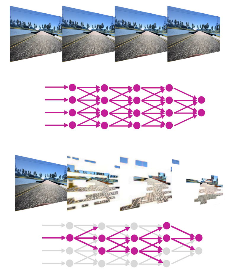 2. Conventional neural networks (top) evaluate all the elements in the model at each level whereas spiking neural networks (bottom) compute only triggered events. (Source: GrAI Matter Labs)
BrainChip’s AKD1000 Neural Network SoC (NSoC) can handle both DNNs and SNNs. The architecture supports up to 80 neural processing units (NPUs)—the AKD1000 has 20 NPUs (Fig. 3). A conversion complex implements a spike event converter and a data-spike event encoder that can handle multivariable digital data as well as preprocessed sensor data. The SNN support only processes non-zero events.
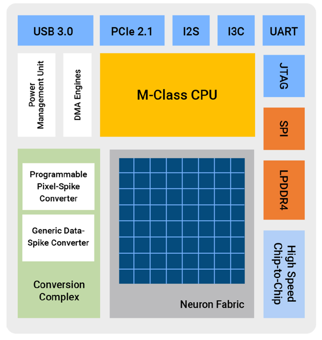 3. The AKD1000 developed by BrainChip neuron fabric supports spiking neural networks. A Cortex-M4 manages system resources.
The AKD1000 benefits from sparsity in both activations and weights. It supports quantizing weights and activations of 1, 2, or 4 bits, leading to a small memory footprint. NPUs communicate events over a mesh network, so model processing doesn’t require external CPU support.
Tenstorrent also targets SNN applications with its Tensix cores (Fig. 4). The cores have five single-issue RISC cores and a 4-TOPS compute engine. A packet processing engine provides decoding/encoding and compression/decompression support along with data-transfer management.
 4. Tenstorrent’s Tensix core is built with five, single-issue RISC codes and a 4-TOPS compute engine.
As with most SNN platforms, Tensix cores can be used on the edge or in the data center. They provide fine-grained conditional execution that makes the system more efficient in processing SNN ML models. The system is designed to scale since it doesn’t use shared memory. It also doesn’t require coherency between nodes, enabling a grid of cores to be efficient connected via its network.
GrAI Matter Labs also targets this event-driven ML approach with its NeuronFlow technology (Fig. 5). The GrAI One consists of 196 neuron cores with 1024 neurons/core, which adds up to 200,704 neurons. A proprietary network-on-chip provides the interconnect. No external DRAM is needed. The SDK includes TensorFlow support.
 5. Events and responses are handled by the network-on-chip (1). The events (2) are then multiplied by the appropriate weights (3), run through the neuron pool (4) and the results are then processed (5).
CNNs, DNNs, and More
Convolutional neural networks are very useful for certain kinds of applications like image classification. SiMaai optimized its chip (Fig. 6) for CNN workloads. By the way, sima means “edge” in Sanskrit. The chip is also ISO 26262 ASIL-B compliant, allowing it to be used in places where other chips aren’t suitable, such as automotive applications.
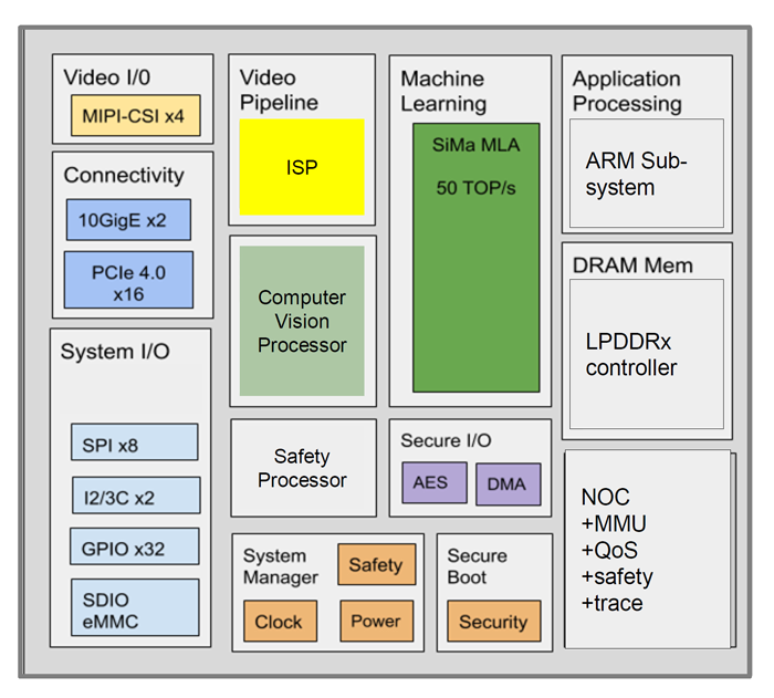 6. SiMaai’s SoC is ISO 26262-compliant. An Arm Cortex provides application support, but it’s augmented with a 50-TOPS machine-learning accelerator (MLA). The MLA includes an image signal processor (ISP) and computer-vision process to preprocess data, allowing all aspects of the system to run on a single chip.
Flex Logix is known for its embedded FPGA technology. The company brought this expertise to the table with its nnMAX design and the InferX X1 coprocessor. The nnMAX array cluster is designed to optimize memory use for weights by implementing Winograd acceleration that handles input and output translation on-the-fly. As a result, the system can remain active, while other solutions are busy moving weights in and out of external memory. The chip supports INT8, INT16, and BFLOAT16. Multiple models can be processed in parallel.
Groq’s Tensor Streaming Processor Chip (TSP) delivers 1 petaoperations per second, running at 1.25 GHz using INT8 values. The chip architecture also enables the system to provide this high level of performance by splitting data and code flow (Fig. 7). The 20 horizontal data-flow superlanes are managed by the vertical SIMD instruction flow. Identical east/west sections let the data flow in both directions. There are 20 superlanes with 16 SIMD units each.
 7. Groq’s chip implements 20 superlanes with 16 SIMD units each. Data flows toward the outer edges of each side, while the control SIMD instructions flow up through the array that’s controlling massive parallel computations. The units within the array include on-chip SRAM (MEM), vector processing engines (VXM), a matrix of MAC cores (MXM), and data reshapers (SXM).
Processors and DSPs
Special ML processors are the order of the day for many new startups, but extending existing architectures garners significant performance benefits while keeping the programming model consistent. This allows for easy integration with the rest of an application.
Cadence’s Tensilica HiFi DSP is now supported by its HiFi Neural Network library in addition to the Nature DSP library that handles vector math like FFT/FIR and IIR computations. The 8-/16-/32-bit SIMD and Vector FPU (VFPU) support provides efficient support for neural networks while enabling a custom design DSP to include customer-specific enhancements.
CEVA’s SensPro sensor hub DSP combines the CEVA-BX2 scalar DSP with a NeuPro AI processor and a CEVA-XM6 vision processor. The wide SIMD processor architecture is configurable to handle 1024 8-×-8 MACs, 256 16-×-16 MACs, or dedicated 8-×-2 binary-neural-network (BNN) support. It can also handle 64 single-precision and 128 half-precision floating-point MACs. This translated to 3 TOPS for the 8-×-8 network’s inferencing, 20 TOPS for BNN inferencing, and 400 GFLOPS for floating-point arithmetic.
The DesignWare ARC HS processor solution developed by Synopsys takes the tack of having lots of processors to address the ML support. This isn’t much different than most solutions, but it’s more along the lines of conventional RISC cores and interconnects that are typically more useful for other applications.
AMD isn’t the only x86 chip producer. Via Technologies has its own x86 IP and its Centaur Technology is making use of that. The x86 platform is integrated with an AI Ncore coprocesessor tied together by a ring (Fig. 8). The Ncore utilizes a very wide SIMD architecture organized into vertical slices to provide a scalable configuration, making future designs more powerful. The chip can deliver 20 TOPS at 2.5 GHz.
 8. Centaur Technology blends x86 processors with the NCore AI accelerator.
I’ve previously covered the Arm Cortex-M55 and Ethos-U55 combination. The Cortex-M55 has an enhanced instruction set that adds a vector pipeline and data path to support the new SIMD instructions. The DSP support includes features like zero overhead loops, circular buffers, and bit reverse addressing.
Still, as with other architectures, a dedicated AI accelerator is being added to the solution—namely, the Ethos-U55 micro network processor unit (microNPU). It supports 8- or 16-bit activations in the models, but internally, weights will always be 8 bits. The microNPU is designed to run autonomously.
While the V in RISC-V doesn’t stand for vectors, SiFive’s latest RISC-V designs do have vector support that’s ideal for neural-network computational support (Fig. 9). What makes this support interesting is that the vector support can be dynamically configured. Vector instructions work with any vector size using vector-length and vector-type registers. The compiler vectorization support takes this into account. The VI2, VI7, and VI8 platforms target every application space through the data center.
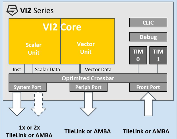 9. SiFive’s RISC-V new designs include configurable vector support.
Extending FPGAs and GPGPUs
Xilinx’s Versal adaptive compute acceleration platform (ACAP) is more than just an FPGA (Fig. 10). The FPGA fabric is at the center, providing low-level customization. However, there are hard cores and an interconnect network surrounding it. The hard cores range from Arm Cortex CPUs for application and real-time chores along with AI and DSP support.
 10. Xilinx’s adaptive compute acceleration platform (ACAP) can incorporate AI engines to complement the FPGA fabric and hardcore Arm Cortex CPUs.
I left Nvidia to the end, as the company announced its A100 platform at the recent, virtual GPU Technology Conference (Fig. 11). This GPGPU incorporates a host of ML enhancements, including sparsity acceleration and multi-instance GPU (MIG) support. The latter provides hardware-based partitioning of the GPU resources that allow more secure and more efficient operation. Large-scale implementations take advantage of the third-generation NVLink and NVSwitch technology that tie multiple devices together.
 11. Nvidia’s Jensen Huang just pulled this motherboard out of the oven. It has eight A100-based GPGPUs specifically designed for AI acceleration.
The plethora of machine-learning options includes more than just the platforms outlined here. They reflect not only the many ways that ML can be accelerated, but also the variety of approaches that are available to developers. Simply choosing a platform can be a major task even when one understands what kind of models will be used, and their possible performance requirements. Likewise, the variants can offer performance differences that are orders of magnitude apart. System and application design has never been more exciting or more complicated. If only we had a machine-learning system to help with that.
"chips" - Google News
May 16, 2020 at 05:59AM
https://ift.tt/3cDGNOJ
Marvell Targets 5G Telecom Gear With New Generation of Chips - Electronic Design
"chips" - Google News
https://ift.tt/2RGyUAH
https://ift.tt/3feFffJ
Bagikan Berita Ini


0 Response to "Marvell Targets 5G Telecom Gear With New Generation of Chips - Electronic Design"
Post a Comment