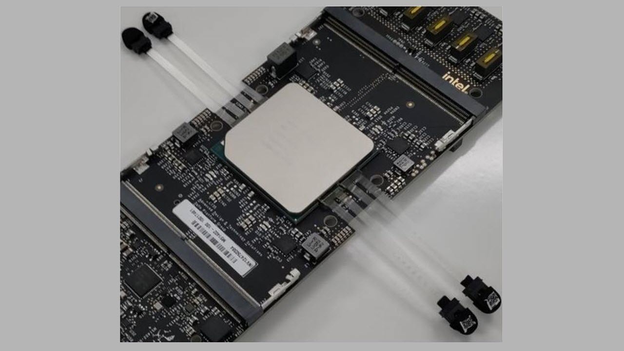
Intel unveiled its first direct mesh-to-mesh photonic fabric at the Hot Chips 2023 chip conference, highlighting its progress towards a future of optical chip-to-chip interconnects that are also championed by the likes of Nvidia and Ayar Labs. However, the eight-core 528-thread chip that Intel used for the demonstration stole the spotlight due to its unique architecture that sports 66 threads per core to enable up to 1TB/s of data throughput. Surprisingly, the chip consumes only 75W of power, with ~60% of the power being used by the optical interconnects, but the design could eventually enable systems with two million cores to be directly connected with under 400ns latency.
Intel's PUMA (Programmable Unified Memory Architecture) chip is part of the DARPA HIVE program that focuses on improving performance in petabyte-scale graph analytics work to unlock a 1000X improvement in performance-per-watt in hyper-sparse workloads.
Surprisingly for an x86-centric company like Intel, the test chip utilizes a custom RISC architecture for streamlined performance in graph analytics workloads, delivering an 8X improvement in single-threaded performance. The chip is also created using TSMC's 7nm process, not Intel's own internal nodes.
After characterizing the target workloads, Intel concluded that it needed to craft an architecture that solved the challenges associated with extreme stress on the memory subsystem, deep pipelines, branch predictors, and out-of-order logic created by the workload.
Intel's custom core employs extreme parallelism to the tune of 66 hardware threads for each of the eight cores, large L1 instruction and data caches, and 4MB of scratchpad SRAM per core. The eight-core chip features 32 optical I/O ports that operate at 32 GB/s/dir apiece, thus totaling 1TB/s of total bandwidth. The chips drop into an eight-socket OCP server sled, offering up to 16 TB/s of total optical throughput for the system, and each chip is fed by 32GB of custom DDR5-4000 DRAM.
Intel fabbed the chip on TSMC's 7nm process with 27.6 billion transistors spanning a 316mm^2 die. The eight cores, which consume 1.2 billion transistors, run down the center of the die, flanked by eight custom memory controllers with an 8-byte access granularity. Communication routers populate the 'empty' center of the chip.
The chip also features four high-speed eight-channel optical I/O chiplets, two each at the top and bottom of the die, that bridge the internal electrical signals to external optical interconnects. These units are connected via Intel's EMIB packaging and use the AIB protocol. The chip also has a PCIe 4.0 x8 connection to communicate with the host system.
Moving the incredible amount of data generated by 528 threads around the die requires an optimized interconnect, so Intel designed a 2D on-die mesh with 16 routers to shuffle data between the cores, memory controllers, and silicon photonics interconnects (eight routers are integrated into the CPU cores, while six routers are dedicated entirely to just data movement).
As you can see in the above album, the photonics connectors are integrated into the chip package and hang off the sides of the chip for external linking to other chips. The chip is connected to an external 'HyperX' optical network that provides all-to-all connections for the individual processing cores. This incredible network allows up to two million cores to be directly connected all-to-all with under 400ns latency.
The end result is impressive — the chip consumes a mere 75W, with 59% of that budget dedicated to silicon photonics and 21% dedicated to the cores. Intel claims the enhanced performance of the optical network allows for nearly perfect linear performance scaling from one to 1000 cores.
The promise of optical interconnects has fueled an intensifying amount of research as the industry looks to future data transport methods that offer superior bandwidth, latency, and power consumption characteristics compared to traditional chip-to-chip communication techniques. While mainstream deployments of optical chip interconnects remain on the horizon, specialized implementations, like those championed by Intel, Nvidia, and Ayar Labs, are nearing readiness for large-scale deployments in the near future.
"chips" - Google News
August 30, 2023 at 10:48PM
https://ift.tt/Ph1k46H
Intel Demos 8-Core, 528-Thread PUMA Chip with 1 TB/s Silicon Photonics - Tom's Hardware
"chips" - Google News
https://ift.tt/y5XATcL
https://ift.tt/6yUjudK
Bagikan Berita Ini


0 Response to "Intel Demos 8-Core, 528-Thread PUMA Chip with 1 TB/s Silicon Photonics - Tom's Hardware"
Post a Comment