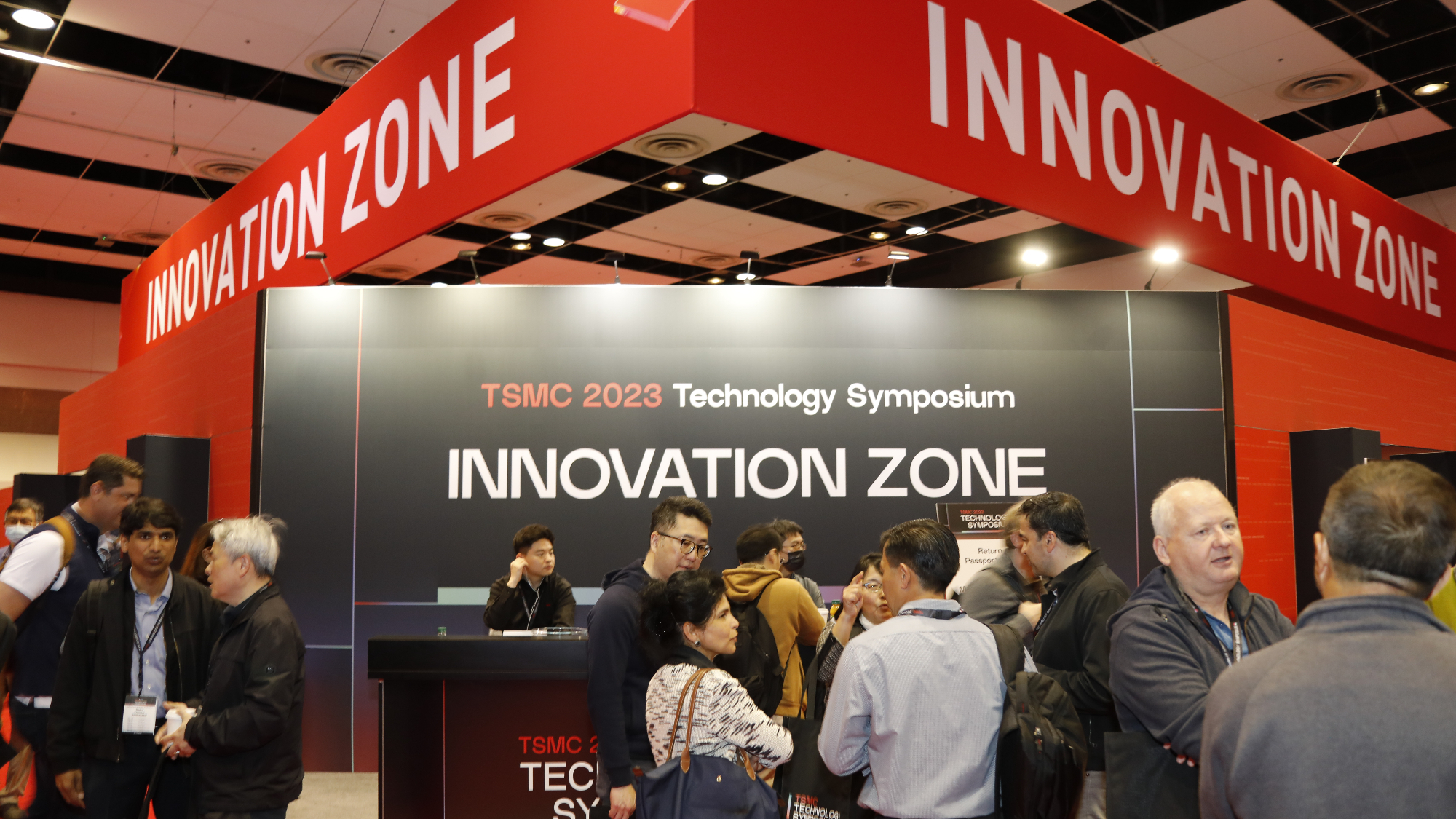
TSMC is developing a new version of its Chip-On-Wafer-On-Substrate-L (CoWoS-L) that will enable it to build extremely large interposers — which it calls Super Carrier Interposers — that pushing the boundaries of current system-in-package (SiPs) sizes to levels never seen before. The next-generation CoWoS technology, planned to be qualified in 2025, will potentially increase the size of interposers up to six reticle sixes, up to 3.3 times what they can do today.
This push for larger chip sizes is driven by the increasing global demand for advanced computing capabilities in applications like artificial intelligence (AI) and high-performance computing (HPC). Major players like AMD, Intel, and Nvidia, are responding to this demand by building highly-complex processors, such as Nvidia's H100, that sell for some $30,000 per unit.
To amplify the computing power of these processors, these companies are using multi-tile chiplet designs: AMD's Instinct 250X/MI300 as well as Intel's Ponte Vecchio that are large and require extremely advanced cooling are among the examples of such designs.
The new version of TSMC's CoWoS-L technology opens new doors by enabling even larger processors to be built. The size of the CoWoS-L technology is massive when considering the theoretical ASML's EUV tool's reticle limit of 858mm^2. With six reticles, these could allow SiPs sized at 5148 mm^2.
But such solutions would not only accommodate a significant number of large compute chiplets, but such devices will require rather tremendous memory subsystems. TSMC is talking about 12 stacks of HBM3/4 memory, which in case of HBM3 means a memory interface with a bandwidth nearing 9.8 TB/s.
However, the construction of such large SiPs is a daunting task with substantial cost implications. To put it in perspective, NVIDIA's H100 accelerator, which is already multiple reticles in size, is priced at about $30,000. Given this, larger and more capable chips developed with the CoWoS-L technology would undoubtedly cost significantly more.
Besides the financial aspect of the chips themselves, there is another major challenge: cooling. The SiPs would be some of the most power-demanding HPC chips yet, which would require advanced cooling systems to prevent overheating. TSMC has been exploring on-chip liquid cooling technology, which has demonstrated its capability to cool silicon packages with power levels up to 2.6 kW. This could potentially handle the cooling requirements of these formidable chips, but it introduces another level of complexity and cost to the process.
"chips" - Google News
May 28, 2023 at 01:39AM
https://ift.tt/i5JS7AH
Pumped Up Procs: TSMC Planning Chips 3x Bigger Than Today - Tom's Hardware
"chips" - Google News
https://ift.tt/S80Q7HX
https://ift.tt/TUqK7x6
Bagikan Berita Ini


0 Response to "Pumped Up Procs: TSMC Planning Chips 3x Bigger Than Today - Tom's Hardware"
Post a Comment